
What do you want to do?
Not sure what to study? Don't worry! You don't need to declare your major until the start of your junior year. Your advisor will be there every step of the way.
Online Graduate Programs
Earn your master's degree online at Wilkes. Our affordable and flexible programs are designed for working professionals just like you.
Pursue your passion or align your graduate studies with your career goals with programs in business administration, creative writing, nursing and education.
At Wilkes, we know you’re capable of more, and we know you’ll achieve it.
We know you're willing to...
Work Hard

Create Connections
Go The Extra Mile
This is a haven for whatever you find interesting. For those willing to work for whatever comes next.
Driven to Make an Impact
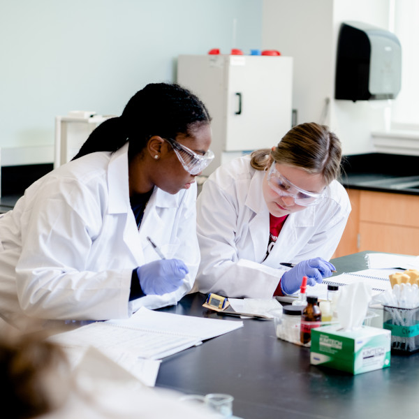
Kahlasia Carter knew she wanted to be part of a nursing program that could match her energy and drive. When thinking about what she wanted to pursue in college, she leaned on the skills that made her come alive – and on areas where she could make a real impact.

Computing a Successful Future
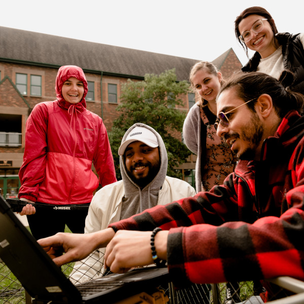
Who do you get when you combine a martial arts expert with an ambitious computer science major? You get Nate Martes, a junior honors student who is also minoring in cloud computing.
Success on Stage, Behind the Scenes and in the Classroom
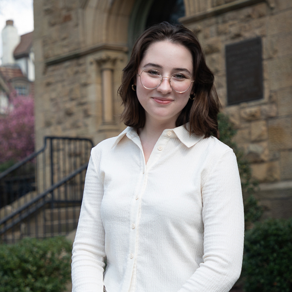
With majors in English and secondary education, as well as minors in theater arts and women’s and gender studies, Madelyn “Maddy” Rex believes that you don’t need to choose just one path to create a future you love. Sometimes, it’s just a matter of aligning the right pieces until they fall into place.
job / graduate school placement rate Asterisk
offered in scholarship aid
student-faculty ratio
An active and vibrant community.
Where Colonels call home.

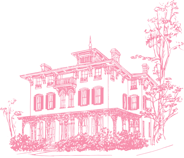
Discover your place at Wilkes. Our compact, 35-acre campus blends stately mansions with state-of-the-art facilities in a historic downtown neighborhood.
When you need a study break, take a walk and enjoy some delicious cuisine from around the world. Visit the River Common Park for a jog, bike ride or picnic. Hop in the car and take advantage of the recreational activities available in the nearby Pocono Mountains. The journey’s up to you.
The leadership opportunities I held within clubs helped me grow as a professional and stand out as a candidate when applying for fellowships.
Kieran Collins - Pharmacy '24, Post-Doctoral Fellow, GSK Medical Affairs

I'm very grateful for my mentors because they trust me as a leader.
Brenda Arias - Bonner Leader

Wilkes has become my home away from home, and I am so happy to be here. I love spreading the word about this amazing school, and I enjoy being involved, sharing my traditions, and learning new ones.
Shanelly Hinds - 2024 President of the International Student Ambassador Club and Secretary of the Wilkes African Cultural Association

You're ready. How will you make it happen?
Our financial aid team will guide you every step of the way. With merit scholarships and financial aid packages for 100% our first-time, full-time domestic students, we’ll show you how to make your Wilkes education a reality.
Connect with #WilkesU
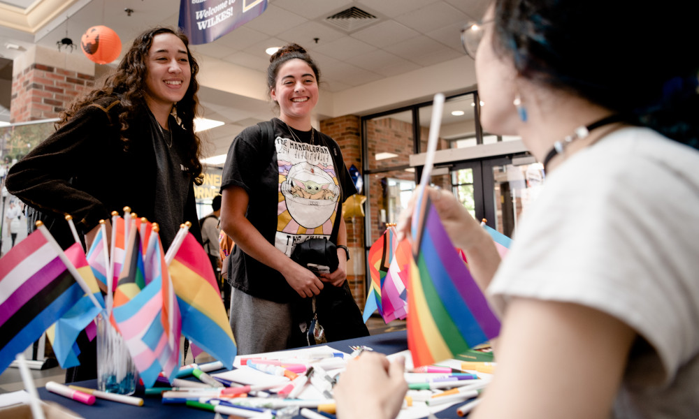
Wilkes welcomes all.
Wilkes University is an inclusive learning environment committed to increasing access to higher education. We create opportunities for the dialogues that increase diversity awareness. We embrace and celebrate diverse backgrounds and perspectives which strengthen and enrich our campus and our community.
What does success look like to you?
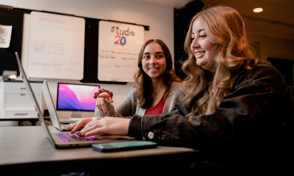
You bring the hard work. We'll provide the support.
Our expert faculty will challenge you to exceed your limits and cheer you on while you do. Focus on research. Start a business. Study abroad. Land an internship. Your success is up to you, but we’ll provide the support to help you get there.
Wilkes is a university that delivers:
- Promise without pretense.
- Access without exception.
- Happiness without compromise.
Are you ready to open the door?
